
Introduction:
Atomic Force Microscope Market Size is expected to grow USD 0.83 Billion by 2032, at (CAGR) of 5.50% during the forecast period (2023 - 2032).
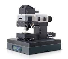
The Atomic Force Microscope (AFM) stands as a pioneering technology in the field of nanoscale imaging and surface analysis. Offering unparalleled resolution and precision, AFMs enable scientists and researchers to explore the atomic and molecular structures of materials with unprecedented detail. As industries and research institutions delve deeper into the realms of nanotechnology, materials science, and biological research, the AFM market continues to witness remarkable growth and innovation.
Analysis of Atomic Force Microscopy:
· Atomic Force Microscopy (AFM) is a powerful imaging technique that utilizes a sharp probe, or tip, to scan the surface of a sample with atomic-scale resolution. The tip interacts with the sample surface, measuring the forces between atoms and generating high-resolution images of surface topography, morphology, and mechanical properties. AFMs can operate in various modes, including contact mode, tapping mode, and non-contact mode, each offering unique advantages for specific applications.
Key Features and Advantages of AFMs:
· High Resolution Imaging: AFMs offer sub-nanometer resolution, allowing researchers to visualize individual atoms and molecules on surfaces with exceptional detail. This capability is invaluable for studying nanoscale structures, surface roughness, and molecular interactions in materials and biological samples.
· Versatility and Multimodal Imaging: AFMs support a wide range of imaging modes and techniques, including topographic imaging, phase imaging, force spectroscopy, and scanning tunneling microscopy (STM). These multimodal capabilities enable researchers to characterize diverse materials and analyze various properties, such as mechanical, electrical, and magnetic properties.
· Non-destructive and Non-invasive: AFM imaging is non-destructive and non-invasive, meaning it does not alter or damage the sample during imaging. This non-invasive nature allows for the imaging of delicate biological samples, polymers, and soft materials without compromising their integrity or functionality.
· Three-dimensional Imaging: AFMs provide three-dimensional imaging capabilities, allowing researchers to reconstruct and visualize surface topography in three dimensions. This 3D imaging capability is essential for understanding the morphology, roughness, and texture of complex surfaces and nanostructures.
· Nanomanipulation and Nanolithography: In addition to imaging, AFMs enable nanomanipulation and nanolithography, allowing researchers to precisely manipulate and fabricate nanostructures on surfaces. These capabilities are essential for applications such as nanofabrication, nanomanipulation, and nanoassembly in nanotechnology and microelectronics.
Atomic Force Microscope Market Trends and Growth Drivers:
· Expansion of Nanotechnology and Materials Science: The growing interest and investment in nanotechnology and materials science drive the demand for advanced imaging and characterization techniques such as AFMs. AFMs play a crucial role in studying nanomaterials, nanostructures, and nanodevices, enabling breakthroughs in areas such as electronics, photonics, energy storage, and biomedicine.
· Biomedical Research and Life Sciences: In biomedical research and life sciences, AFMs are utilized for imaging and analyzing biological samples such as cells, tissues, proteins, and DNA. AFM imaging provides valuable insights into cellular structures, membrane properties, and biomolecular interactions, contributing to advancements in drug discovery, regenerative medicine, and disease diagnostics.
· Semiconductor and Microelectronics Industry: The semiconductor and microelectronics industry relies on AFMs for inspecting semiconductor materials, thin films, and device structures with nanoscale precision. AFMs play a crucial role in quality control, defect analysis, and process optimization in semiconductor fabrication facilities, ensuring the reliability and performance of microelectronic devices.
· Environmental and Energy Applications: AFMs are used in environmental and energy applications for studying nanomaterials, catalysts, and energy storage materials. Researchers utilize AFMs to investigate the surface properties, reactivity, and performance of materials in areas such as environmental remediation, renewable energy, and fuel cells.
· Educational and Academic Research: AFMs are widely used in educational institutions and academic research laboratories for teaching, training, and fundamental research in physics, chemistry, biology, and engineering. The accessibility and versatility of AFM systems empower students and researchers to explore nanoscience and nanotechnology concepts and conduct cutting-edge research in their respective fields.
Get a free sample @ https://www.marketresearchfuture.com/sample_request/12459
Key Companies in the Atomic Force Microscope market include:
· Concept Scientific Instruments
· Advanced Technologies Center
· WITec (Wissenschaftliche Instrumente und Technologie GmbH)
· Park Systems, Anton Paar
· AFM Workshop
· Hitachi High-Technologies Corp (HHT)
· Semilab Inc.
· Bruker Corporation
· Nanomagnetics Instruments
· Nanosurf AG
· Nanonics Imaging Ltd
· Attocube Systems AG
· NT-MDT Spectrum Instruments
· Oxford Instruments
· HORIBA, Ltd.
Challenges and Opportunities
While the AFM market share presents significant growth opportunities, it also faces challenges such as:
· Cost and Complexity: The high cost and complexity of AFM systems pose barriers to adoption, particularly for small research laboratories and educational institutions with limited budgets and resources. Manufacturers must innovate and develop more affordable, user-friendly AFM solutions to broaden access and accelerate adoption.
· Sample Preparation and Handling: Sample preparation and handling are critical considerations in AFM imaging, as sample quality and cleanliness directly impact imaging results. Proper sample preparation techniques, such as surface cleaning, mounting, and immobilization, are essential for obtaining accurate and reliable AFM images.
· Data Analysis and Interpretation: AFM imaging generates large datasets that require sophisticated data analysis and interpretation tools for extracting meaningful information. Researchers must possess the expertise and computational resources to analyze AFM images, quantify surface features, and interpret structural and mechanical properties accurately.
· Instrument Calibration and Maintenance: AFM systems require regular calibration, maintenance, and troubleshooting to ensure optimal performance and reliability. Manufacturers and users must invest in training, technical support, and preventive maintenance programs to maximize the lifespan and productivity of AFM equipment.
· Integration with Multimodal Techniques: Integrating AFM with complementary imaging and analytical techniques, such as scanning electron microscopy (SEM), transmission electron microscopy (TEM), and spectroscopy, presents opportunities for synergistic analysis and correlative imaging. Manufacturers and researchers must explore integrated imaging platforms and workflows to leverage the strengths of each technique and address the limitations of standalone AFM systems.
Get a regional report on US Atomic Force Microscope Market