Introduction:
GaAs wafer market size is expected to grow USD 1.39 billion by 2032, at (CAGR) of 12.00% during the forecast period (2023 - 2032).
In the realm of semiconductor materials, gallium arsenide (GaAs) wafers have emerged as key players, driving innovation and technological advancement in various industries. With their unique properties and versatile applications, GaAs wafers have captured the attention of researchers, manufacturers, and investors alike, fueling the growth of the GaAs wafer market.
Understanding GaAs Wafers:
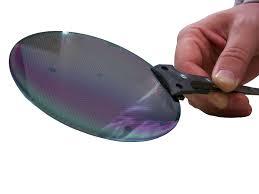
GaAs wafers are semiconductor substrates made from gallium arsenide, a compound of gallium and arsenic. These wafers possess exceptional properties that make them ideal for a wide range of electronic and optoelectronic applications. Compared to traditional silicon wafers, GaAs wafers offer higher electron mobility, faster switching speeds, and better performance at high frequencies, making them indispensable in fields such as telecommunications, aerospace, and photovoltaics.
Driving Forces Behind Market Growth:
Several factors contribute to the burgeoning demand for GaAs wafers:
· Rising Demand for High-Speed Communication: With the proliferation of data-intensive applications such as 5G networks, internet of things (IoT) devices, and cloud computing, there is an increasing need for high-speed, high-frequency electronic components. GaAs wafers play a crucial role in the fabrication of high-performance RF (radio frequency) and microwave devices used in telecommunications infrastructure.
· Expansion of the Aerospace and Defense Sector: GaAs-based components are widely used in radar systems, satellite communications, and missile guidance systems due to their ability to operate reliably in harsh environments and at elevated temperatures. As governments worldwide continue to invest in defense modernization and space exploration initiatives, the demand for GaAs wafers is expected to remain robust.
· Growing Adoption in Photonic Devices: GaAs wafers are also utilized in the production of optoelectronic devices such as LEDs (light-emitting diodes), laser diodes, and solar cells. The superior optical properties of GaAs, including its direct bandgap and high photon absorption coefficient, make it well-suited for applications requiring efficient light emission or absorption.
Market Challenges and Opportunities:
· While the GaAs wafer market presents significant growth prospects, it is not without its challenges. The production of GaAs wafers involves complex manufacturing processes and requires specialized equipment and expertise, leading to higher manufacturing costs compared to silicon wafers. Additionally, fluctuations in raw material prices and supply chain disruptions can impact market dynamics.
· However, advancements in epitaxial growth techniques, such as molecular beam epitaxy (MBE) and metalorganic chemical vapor deposition (MOCVD), have led to improvements in wafer quality, yield, and scalability, thereby mitigating some of these challenges. Moreover, ongoing research and development efforts aimed at enhancing GaAs-based devices' performance and reducing production costs are poised to unlock new opportunities for market growth.
Get a free sample @ https://www.marketresearchfuture.com/sample_request/6473
Key Companies in the GaAs Wafer market include:
· Semiconductor Wafer Inc (Taiwan)
· AXT, Inc. (U.S.)
· Freiberger Compound Materials GmbH (Germany)
· Xiamen Powerway Advanced Material Co., Ltd. (China)
· Sumitomo Electric Industries, Ltd. (Japan)
· Wafer Technology Ltd. (U.K.)
· MTI Corporation (U.S.)
· Vital Materials Co., Limited. (China)
· DOWA Electronics Materials Co., Ltd. (Japan)
· II-VI Incorporated (U.S.)
· IQE PLC (U.K.)
Future Outlook:
As technological advancements continue to drive innovation across various industries, the demand for GaAs wafers is expected to witness steady growth in the coming years. Emerging applications such as automotive radar, virtual reality (VR) systems, and advanced driver-assistance systems (ADAS) are projected to further expand the GaAs wafer market's reach.